- 您现在的位置:买卖IC网 > Sheet目录1991 > CS4362-KQZ (Cirrus Logic Inc)IC DAC 6CH 114DB 192KHZ 48LQFP
6
DS257F2
CS4362
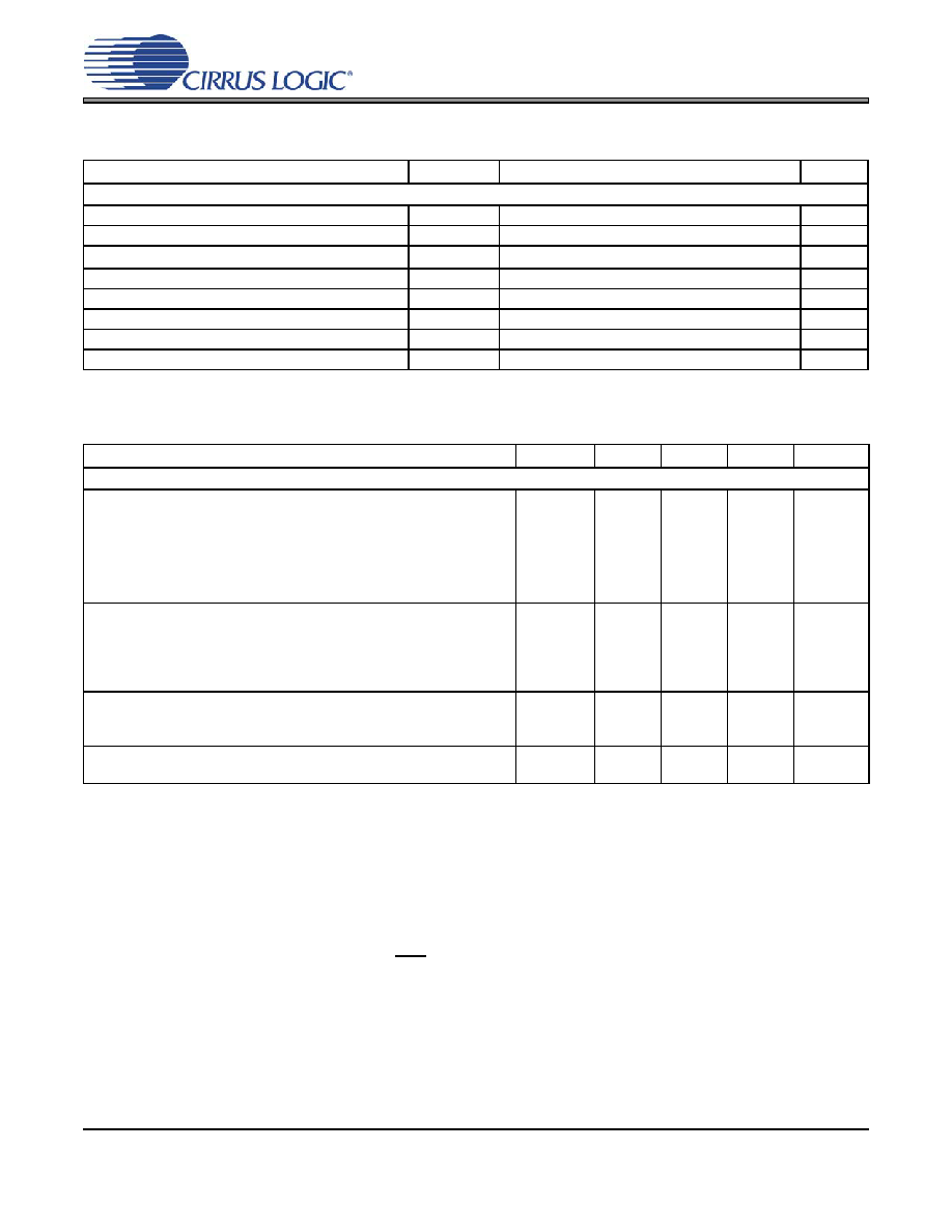
ANALOG CHARACTERISTICS
(Continued)
POWER AND THERMAL CHARACTERISTICS
Notes:
4.
VFS is tested under load RL and includes attenuation due to ZOUT
5.
Current consumption increases with increasing FS within a given speed mode and is signal dependant.
Max values are based on highest FS and highest MCLK.
6.
ILC measured with no external loading on the SDA pin.
7.
This specification is violated when the VLC supply is greater than VD and when pin 16 (M1/SDA) is tied
or pulled low. Logic tied to pin 16 needs to be able to sink this current.
8.
Power Down Mode is defined as RST pin = Low with all clock and data lines held static.
9.
Parameters
Symbol
Min
Typ
Max
Units
Analog Output - All PCM modes and DSD
Full Scale Differential Output Voltage
VFS
86% VA
91% VA
96% VA
Vpp
Quiescent Voltage
VQ
-
50% VA
-VDC
Max Current from VQ
IQMAX
-1
-
μA
Interchannel Gain Mismatch
-
0.1
-
dB
Gain Drift
-
100
-
ppm/°C
Output Impedance
ZOUT
-
100
-
Ω
AC-Load Resistance
RL
3-
-
k
Ω
Load Capacitance
CL
-
100
pF
Parameters
Symbol
Min
Typ
Max
Units
Power Supplies
Power Supply Current
normal operation, VA= 5 V
VD= 5 V
VD= 3.3 V
VLS=5 V
power-down state (all supplies) (Note 8)
IA
ID
ILC
ILS
Ipd
-
50
38
25
2
84
200
55
60
40
-
mA
μA
Power Dissipation
VA = 5 V, VD = 3.3 V
normal operation
power-down (Note 8)
VA = 5 V, VD = 5 V
normal operation
power-down (Note 8)
-
335
1
440
1
410
-
575
-
mW
Package Thermal Resistance
multi-layer
dual-layer
θ
JA
θ
JA
θ
JC
-
48
65
15
-
°C/Watt
Power Supply Rejection Ratio (Note 9)
(1 kHz)
(60 Hz)
PSRR
-
60
40
-
dB
发布紧急采购,3分钟左右您将得到回复。
相关PDF资料
CS4362A-DQZ
IC DAC 6CH 114DB 192KHZ 48-LQFP
CS4364-CQZR
IC DAC 103DB 24BIT 6CH 48-LQFP
CS4382A-DQZ
IC DAC 8CH 114DB 192KHZ 48-LQFP
CS4384-CQZR
IC DAC 8CH 103DB 192KHZ 48-LQFP
CS4385-DQZR
IC DAC 8CH 114DB 192KHZ 48-LQFP
CS4391A-KZZR
IC DAC 24BIT 192KHZ W/VC 20TSSOP
CS4392-KZZ
IC DAC 24BIT 192KHZ W/VC 20TSSOP
CS4397-KSZ
IC DAC 24BIT MULTY STNDRD 28SOIC
相关代理商/技术参数
CS4362-KQZR
功能描述:数模转换器- DAC IC 114dB 192kHz 6Ch DAC RoHS:否 制造商:Texas Instruments 转换器数量:1 DAC 输出端数量:1 转换速率:2 MSPs 分辨率:16 bit 接口类型:QSPI, SPI, Serial (3-Wire, Microwire) 稳定时间:1 us 最大工作温度:+ 85 C 安装风格:SMD/SMT 封装 / 箱体:SOIC-14 封装:Tube
CS4364
制造商:CIRRUS 制造商全称:Cirrus Logic 功能描述:103 dB, 192 kHz 6-Channel D/A Converter
CS4364_08
制造商:CIRRUS 制造商全称:Cirrus Logic 功能描述:103 dB, 192 kHz 6-Channel D/A Converter
CS4364-CQZ
功能描述:数模转换器- DAC IC 24bit 6Chn DAC w/ DSD Supt&Lw-Ltnc DF RoHS:否 制造商:Texas Instruments 转换器数量:1 DAC 输出端数量:1 转换速率:2 MSPs 分辨率:16 bit 接口类型:QSPI, SPI, Serial (3-Wire, Microwire) 稳定时间:1 us 最大工作温度:+ 85 C 安装风格:SMD/SMT 封装 / 箱体:SOIC-14 封装:Tube
CS4364-CQZR
功能描述:数模转换器- DAC IC 24b 6Ch DAC w/DSD Supt/Lw-Ltnc DF RoHS:否 制造商:Texas Instruments 转换器数量:1 DAC 输出端数量:1 转换速率:2 MSPs 分辨率:16 bit 接口类型:QSPI, SPI, Serial (3-Wire, Microwire) 稳定时间:1 us 最大工作温度:+ 85 C 安装风格:SMD/SMT 封装 / 箱体:SOIC-14 封装:Tube
CS4364-DQZ
制造商:CIRRUS 制造商全称:Cirrus Logic 功能描述:103 dB, 192 kHz 6-Channel D/A Converter
CS4364-DQZR
制造商:CIRRUS 制造商全称:Cirrus Logic 功能描述:103 dB, 192 kHz 6-Channel D/A Converter
CS4365
制造商:CIRRUS 制造商全称:Cirrus Logic 功能描述:114 dB, 192 kHz 6-Channel D/A Converter